Sep 24 2019

M36 meeting

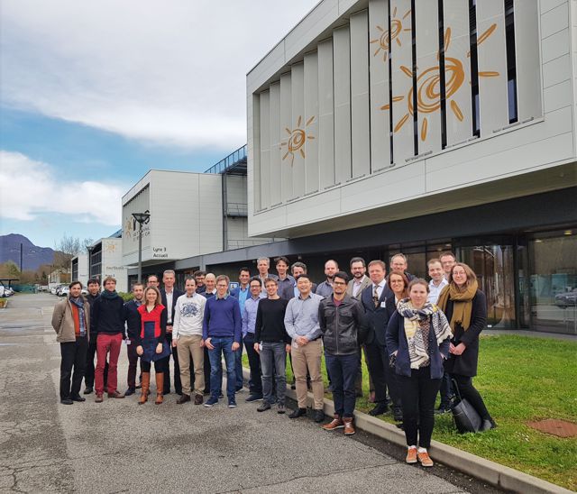
The final general assembly meeting at the end of month 36 was hosted by CEA-INES in Chambery, France on Sep 24 2019. The effort of the consortium members during the last six months was focused in pushing the limits to reach the project goals. The most important highlights are:

  • Completion of the second round robin on TCO and carrier selective junction layers.
  • High mobility ITO (90 – 100 cm²/Vs) layers were obtained after annealing.
  • Optimized plating route with AZO as TCO yielded 21.8% cell efficiency with 79.8% FF.
  • Simplified plating route without resist mask based on selective plating yielded 21.2% cell efficiency which is very close to the precursor limit.

During this period, 3 papers were published in scientific journals and there were 14 presentations in 5 conferences and workshops:

  • Metallization & Interconnection Workshop 2019: 1 visual
  • ETIP PV - Readying for the TW era: 1 visual
  • IEEE PVSC 2019: 2 oral
  • EU PVSEC 2019: 4 oral, 3 visual
  • High Efficiency Approaches in c-Si PV Workshop: 3 oral
Apr 19 2019

M30 meeting

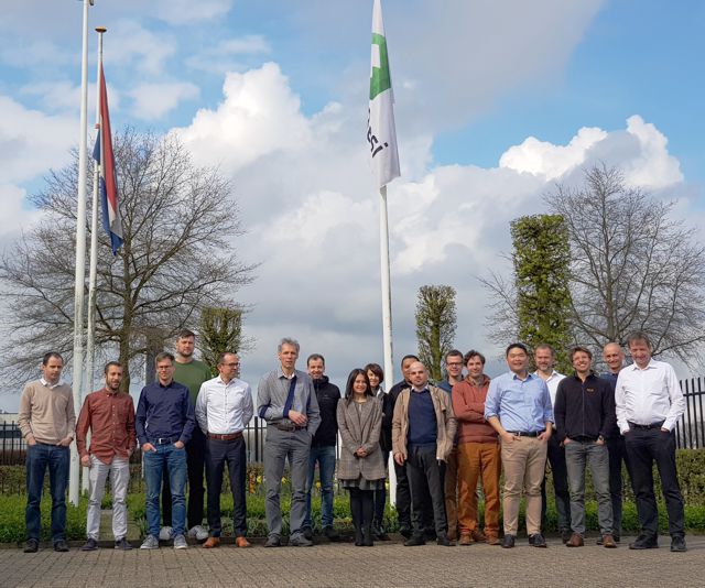
The general assembly meeting at month 30 was hosted by MECO in Drunen, The Netherlands on Apr 2-3 2019. Most of the effort in this project period was put into integration of different components with supporting research and development from base work packages. The most important highlights are:

  • First large-area plated carrier selective junction solar cell with efficiency above 20% was produced using simplified process sequence avoiding resist mask
  • High-throughput plating route was organized between five partners and samples are almost complete
  • Hydrogenated TCO followed by annealing provides a promising option for hydrogenation of the poly-Si layer without additional manufacturing step
  • Development of a new measurement procedure for improved characterization of performance losses during dicing processes
  • Developed selective contacts are also suitable for future perovskite-silicon tandem solar cells.

During this period, 2 papers were published in scientific journals, and several abstracts were submitted to forthcoming conferences.

Oct 16 2018

M24 meeting

Entering into the third year of the DISC project, the STC meeting after 24 months of the project was held at Fraunhofer ISE in Freiburg, Germany on Oct 15-16 2018. The development-phase work packages are finalizing their solutions and making them ready to work together in the integration phase. Simultaneously, in the integration phase the first common cell prototype was developed.

Highlights of the last 6 months include:

  • First application of electroplating metallization on In free layer (PVD AZO) leading to 20.9% solar cell efficiency.
  • New Round Robin combining optimized CSJs and TCO layers is on going and is focusing on device relevant layers.
  • Simulation based loss analysis for transparent metal compound based carrier selective contacts.
  • Printed contact fingers with width below 30 μm and conductivity below 5∙10-7 ohm∙m were realized, enabling low series resistance and low shading for the DISC solar cell.
  • Meco’s plating tool-manufacturing site was visited and the relevant data for LCA and cost calculation was obtained.
  • The first common cell integration of CSJ, TCO, and metallization developed in WP1, 2, and 3 led to achievement of a 21.2% solar cell featuring poly-Si CSJ on front and back side.

Dissemination activities in the last 6 months include 4 published papers in scientific journals and 15 participations in 4 international conferences:

  • EUPVSEC 2018: 1 plenary, 6 oral, 1 poster, 1 parallel
  • WCPEC-7: 4 oral
  • ETIP PV: 1 poster
  • MRS Spring Meeting 2018; 1 oral
Apr 27 2018

M18 meeting

In the middle of the project's timeline, after 18 months the STC meeting was held at CEA Ines in Chambery, France on Apr 11-12 2018. Significant scientific progress was made in the core work packages during the third reporting period, enabling the project to enter the integration phase in the next reporting period. These 6 months’ highlights include:

  • Project-wide round robin of TCO/CSJ samples generated crucial data for the project:
    • the effect of TCO deposition on passivation that led to the conclusion of the necessity to develop low-damage TCO processes,
    • the complete and advanced characterization of all tested TCOs that helped to better understand conduction mechanisms.
  • The next generation smart wire interconnection technology lead to 2.63% relative increase in module efficiency and 2% lower performance loss after double IEC 612015 damp heat thermal cycling.
  • LCA data collection started by site visits and a questionnaire.
  • Development of the simulation model for raytracing analysis of smart-wire modules.
  • Evaluation of the optimal approach for the half cutting process.

Scientific output of the project within the last 6 months includes 4 papers in renown scientific journals as well as participation in three international conferences:

Sep 1 2017

M12 meeting

STC meeting after 12 months since the project’s start took place at ISFH in Hameln on Aug 30-31 2017. The project is in full swing in and is focused to reach the anticipated goals. The most important highlights from last 6 months are:

  • Demonstration of recombination current densities around 5 fA/cm2 for electron- and hole-selective contacts on textured and planar surfaces, respectively. Application on the full area p-type c-Si solar cells results in efficiency above 22%.
  • Further development of both high-performance In-based TCOs and low-cost Zn-based. Studies on several TCO/CSJ contacts showing low contact resistance (< 0.1 Ω cm2).
  • Development of Cu plating approach with excellent contacting properties (rc < 0.16 mΩ∙cm2; fingers: σ > 3.7∙107 S/m, w < 30 µm, h > 15 µm) maintain VOC > 730 mV leading to 83% FF on front and rear plated 6” CZ-Si precursors with TCO.
  • Verification of transparency dependence on deposition temperatures of poly-Si.
    Development of 3D simulation model for TLM measurement with complex structure geometry.
    Structural investigation of the impact of annealing step on TCO stacks.

Initial results were already presented at the SiliconPV 2017 conference with three scientific contributions.

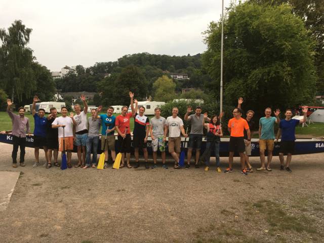
During the fruitful and constructive M12 meeting, the consortium members also proved team spirit in other disciplines. We successfully rowed the Weser river!

Mar 30 2017

M6 meeting

An official project meeting after 6 months of the project was held in Lyon, France. The event was attended by over 25 representatives of all 13 consortium partners. Recent project developments were discussed. Work package leaders presented the work done within the work packages. All work packages were reported to be on track with already encouraging preliminary results.

Highlights:

  • Development of electron-and hole-selective junctions for textured surfaces, attaining recombination current densities below 5 fA/cm2 and 30 fA/cm2, respectively.
  • Low-damage deposition (ALD) of In-based TCO layers with high mobility (70 cm2/V/s) and ALD of low-cost Zn-based TCO layers.
  • In-free SmartWire interconnection.
  • Quantification of free carrier absorption losses by experiment and simulation.
    I-V characteristics at deep temperatures of solar cells featuring polysilicon-based passivating contacts
    Optical simulation study of the impact of different O2 amount during ITO deposition
  • Design of project identity set and launch of public DISC website.
Oct 4 2016

Kick-off meeting

A DISC project kick-off meeting has been held on Oct 4 2016 in Brussels. The entire project consortium led by the coordinator, Institut für Solarenergieforschung Hameln (ISFH), supported by a project management specialist, Ayming, and The European Commission represented by the Innovation and Networks Executive Agency (INEA) have officially launched the DISC project as of Oct 1 2016.

Read the public announcement here.